- 您现在的位置:买卖IC网 > Sheet目录527 > SUM90N10-8M2P-E3 (Vishay Siliconix)MOSFET N-CH D-S 100V D2PAK
SUM90N10-8m2P
Vishay Siliconix
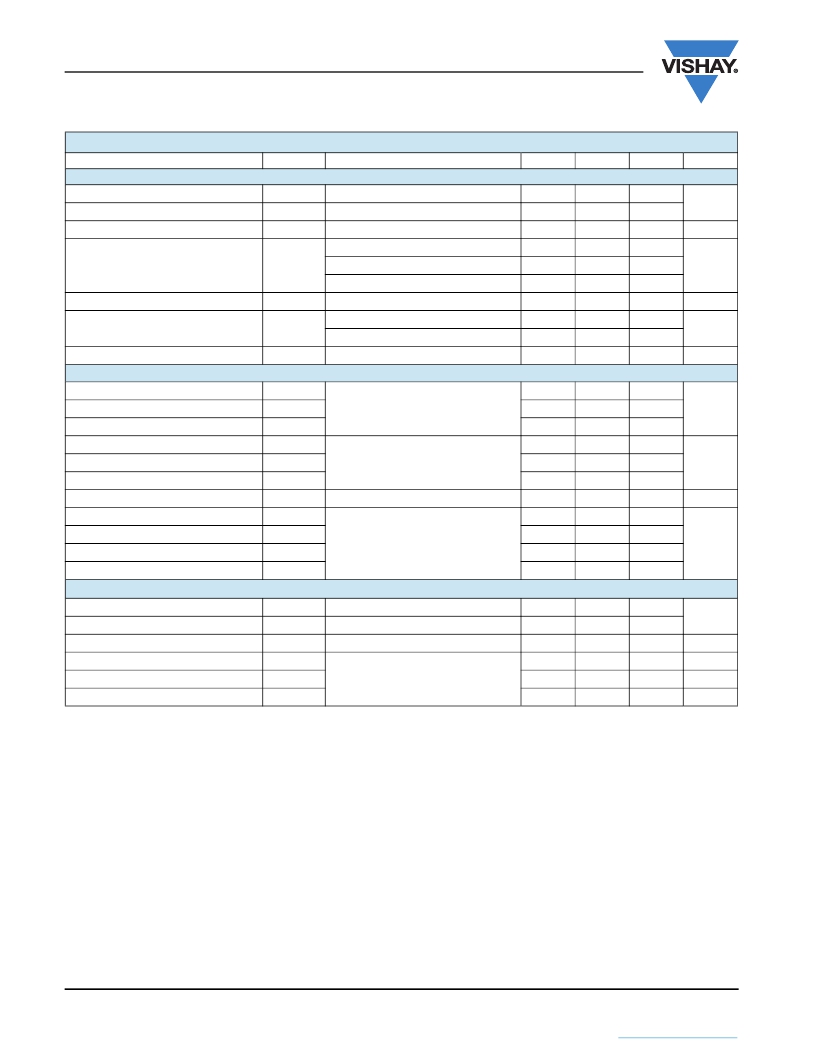
SPECIFICATIONS (T J = 25 °C, unless otherwise noted)
Parameter
Symbol
Test Conditions
Min.
Typ.
Max.
Unit
Static
Drain-Source Breakdown Voltage
Gate Threshold Voltage
Gate-Body Leakage
V (BR)DSS
V GS(th)
I GSS
V DS = 0 V, I D = 250 μA
V DS = V GS , I D = 250 μA
V DS = 0 V, V GS = ± 20 V
100
2.5
4.5
± 250
V
nA
V DS = 100 V, V GS = 0 V
1
Zero Gate Voltage Drain Current
I DSS
V DS = 100 V, V GS = 0 V, T J = 125 °C
50
μA
V DS = 100 V, V GS = 0 V, T J = 150 °C
250
On-State Drain Current a
I D(on)
V DS ?? 10 V, V GS = 10 V
70
A
Drain-Source On-State Resistance a
Forward Transconductance a
R DS(on)
g fs
V GS = 10 V, I D = 20 A
V GS = 10 V, I D = 20 A, T J = 125 °C
V DS = 15 V, I D = 20 A
0.0067
0.0127
62
0.0082
0.0170
?
S
Dynamic b
Input Capacitance
C iss
6290
Output Capacitance
Reverse Transfer Capacitance
Total Gate Charge c
C oss
C rss
Q g
V GS = 0 V, V DS = 50 V, f = 1 MHz
535
182
97
150
pF
Gate-Source
Charge c
Q gs
V DS = 50 V, V GS = 10 V, I D = 85 A
32
nC
Gate-Drain Charge c
Q gd
25
Gate Resistance
Turn-On Delay Time
c
R g
t d(on)
f = 1 MHz
0.28
1.4
23
2.8
35
?
Rise Time c
Turn-Off Delay Time
c
t r
t d(off)
V DD = 50 V, R L = 0.588 ?
I D ? 85 A, V GEN = 10 V, R g = 1 ?
17
34
26
52
ns
Fall Time c
t f
9
18
Source-Drain Diode Ratings and Characteristics (T C = 25 °C)
b
Continuous Current
Pulsed Current
I S
I SM
85
240
A
Forward Voltage a
Reverse Recovery Time
Peak Reverse Recovery Current
Reverse Recovery Charge
V SD
t rr
I RM(REC)
Q rr
I F = 30 A, V GS = 0 V
I F = 75 A, di/dt = 100 A/μs
0.85
61
3
91
1.5
100
4.5
130
V
ns
A
μC
Notes:
a. Pulse test; pulse width ? 300 μs, duty cycle ? 2 %.
b. Guaranteed by design, not subject to production testing.
c. Independent of operating temperature.
Stresses beyond those listed under “Absolute Maximum Ratings” may cause permanent damage to the device. These are stress ratings only, and functional operation
of the device at these or any other conditions beyond those indicated in the operational sections of the specifications is not implied. Exposure to absolute maximum
rating conditions for extended periods may affect device reliability.
www.vishay.com
2
Document Number: 74643
S12-0335-Rev. B, 13-Feb-12
This document is subject to change without notice.
THE PRODUCTS DESCRIBED HEREIN AND THIS DOCUMENT ARE SUBJECT TO SPECIFIC DISCLAIMERS, SET FORTH AT www.vishay.com/doc?91000
发布紧急采购,3分钟左右您将得到回复。
相关PDF资料
SUP18N15-95-E3
MOSFET N-CH 150V 18A TO220-3
SUP28N15-52-E3
MOSFET N-CH D-S 150V TO220AB
SUP40P10-43-GE3
MOSFET P-CH 100V 36A TO220AB
SUP45N03-13L-E3
MOSFET N-CH D-S 30V TO220AB
SUP60N02-4M5P-E3
MOSFET N-CH D-S 20V TO220AB
SUP60N10-16L-E3
MOSFET N-CH D-S 100V TO220AB
SUP60N10-18P-E3
MOSFET N-CH D-S 100V TO220AB
SUP65P04-15-E3
MOSFET P-CH 40V 65A TO220AB
相关代理商/技术参数
SUM90P10-19-E3
功能描述:MOSFET 100V 90A 375W 19mohm @ 10V RoHS:否 制造商:STMicroelectronics 晶体管极性:N-Channel 汲极/源极击穿电压:650 V 闸/源击穿电压:25 V 漏极连续电流:130 A 电阻汲极/源极 RDS(导通):0.014 Ohms 配置:Single 最大工作温度: 安装风格:Through Hole 封装 / 箱体:Max247 封装:Tube
SUM90P10-19L
制造商:VISHAY 制造商全称:Vishay Siliconix 功能描述:P-Channel 100-V (D-S) MOSFET
SUM90P10-19L_08
制造商:VISHAY 制造商全称:Vishay Siliconix 功能描述:P-Channel 100-V (D-S) MOSFET
SUM90P10-19L-E3
功能描述:MOSFET 100V 90A 375W 19mohm @ 10V RoHS:否 制造商:STMicroelectronics 晶体管极性:N-Channel 汲极/源极击穿电压:650 V 闸/源击穿电压:25 V 漏极连续电流:130 A 电阻汲极/源极 RDS(导通):0.014 Ohms 配置:Single 最大工作温度: 安装风格:Through Hole 封装 / 箱体:Max247 封装:Tube
SUM90P10-19L-E3
制造商:Vishay Siliconix 功能描述:P CHANNEL MOSFET, -100V, 90A TO-263
SUM90UF
制造商:SSDI 制造商全称:Solid States Devices, Inc 功能描述:400 mA 6,000 thru 9,000 VOLTS 60 ns ULTRA FAST RECOVERY RECTIFIER
SUM90UFSMS
制造商:SSDI 制造商全称:Solid States Devices, Inc 功能描述:400 mA 6,000 thru 9,000 VOLTS 60 ns ULTRA FAST RECOVERY RECTIFIER
SUMIL25
制造商:STMicroelectronics 功能描述:SD4013 - Bulk
